|
ADI公司的AD7685是16位電荷重新分布逐次逼近模數轉換器(ADC),單電源2.3V-5.5V工作,包括有不丟失碼的低功耗高速16位取樣ADC,內部轉換時鐘,以及多功能串口.吞吐量250kSPS, INL典型為±0.6 LSB,最大為±2 LSB((±0.003% of FSR)),20kHz的SINAD為93.5dB,THD為-110dB,假性差分模擬輸入,主要用在手持設備,醫療儀器,移動通信,PDA,數據采集和儀器儀表于過程控制.本文介紹了AD7685主要特性, 多個電源應用電源框圖, 真正16位隔離同時取樣采集系統框圖,EVAL-AD76XXCB 8/10-Pin評估板主要特性,電路圖以及完整的過程控制用高速高CMRR精密模擬前端簡化框圖, EVAL-A-INPUT-1AZ評估板電路圖和材料清單. The AD7685 is a 16-bit, charge redistribution successive approximation, analog-to-digital converter (ADC) that operates from a single power supply, VDD, between 2.3 V to 5.5 V. It contains a low power, high speed, 16-bit sampling ADC with no missing codes, an internal conversion clock, and a versatile serial interface port. The part also contains a low noise, wide bandwidth, short aperture delay, track-and-hold circuit. On the CNV rising edge, it samples an analog input IN+ between 0 V to REF with respect to a ground sense IN−. The reference voltage, REF, is applied externally and can be set up to the supply voltage. Power dissipation scales linearly with throughput. The SPI-compatible serial interface also features the ability, using the SDI input, to daisy chain several ADCs on a single 3-wire bus or provides an optional BUSY indicator. It is compatible with 1.8 V, 2.5 V, 3 V, or 5 V logic using the separate supply VIO. The AD7685 is housed in a 10-lead MSOP or a 10-lead QFN (LFCSP) with operation specified from −40°C to +85°C. AD7685主要特性: 16-bit resolution with no missing codes Throughput: 250 kSPS INL: ±0.6 LSB typical, ±2 LSB maximum (±0.003% of FSR) SINAD: 93.5 dB @ 20 kHz THD: −110 dB @ 20 kHz Pseudo differential analog input range 0 V to VREF with VREF up to VDD No pipeline delay Single-supply operation 2.3 V to 5.5 V with 1.8 V to 5 V logic interface Serial interface SPI®-/QSPI™-/MICROWIRE™-/DSP-compatible Daisy-chain multiple ADCs, BUSY indicator Power dissipation 1.4 μW @ 2.5 V/100 SPS 1.35 mW @ 2.5 V/100 kSPS, 4 mW @ 5 V/100 kSPS Standby current: 1 nA 10-lead package: MSOP (MSOP-8 size) and 3 mm × 3 mm QFN (LFCSP) (SOT-23 size) Pin-for-pin-compatible with 10-lead MSOP/QFN PulSAR® ADCs AD7685應用: Battery-powered equipment Medical instruments Mobile communications Personal digital assistants (PDAs) Data acquisition Instrumentation Process controls 
圖1.ADC簡化電路圖
圖2.AD7685 多個電源應用電源框圖
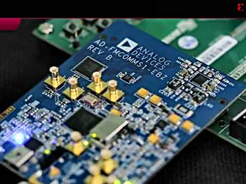
圖3.AD7685真正16位隔離同時取樣采集系統框圖 EVAL-AD76XXCB 8/10-Pin評估板 The EVAL-AD76XXCB 8/10-Pin is an evaluation board for the AD768x/AD769x/AD794x/AD798x 8 and 10-pin PulSAR high resolution ADCs (see the Ordering Guide at the end of this document for a product list). The evaluation board is designed to demonstrate the ADC’s performance and to provide an easy to understand interface for a variety of system applications. The evaluation board is ideal for use with either Analog Devices EVAL-CONTROL BRD2/BRD3 (EVAL-CONTROL BRDx), DSP based controller board, to run the Analog devices evaluation software and to develop a specific application using LabVIEW, or as a stand-alone evaluation board. The EVAL-CONTROL BRDx is sold separately from the evaluation board, is required to run the evaluation software, is not required in stand alone mode and can be reused with many Analog Devices ADCs. EVAL-AD76XXCB 8/10-Pin評估板主要特性: Versatile analog signal conditioning circuitry On-board reference, crystal oscillator and buffers 16-bit Parallel Buffered Outputs Ideal for DSP and data acquisition card interfaces Analog and digital prototyping area for breadbording the target system Stand-alone operation or Eval control board compatibility PC software for control and data analysis LabVIEW1 driver to develop custom application
圖4. EVAL-AD76XXCB 8/10-Pin評估板電路圖:模擬部分
圖5. EVAL-AD76XXCB 8/10-Pin評估板電路圖:數字部分
圖6. EVAL-AD76XXCB 8/10-Pin評估板電路圖:電源部分
圖7. EVAL-AD76XXCB 8/10-Pin評估板電路圖:選擇部分 完整的過程控制用高速高CMRR精密模擬前端 Complete High Speed, High CMRR Precision Analog Front End for Process Control Signal levels in industrial process control systems generally fall into one of the following categories: single-ended current (4 mA-to-20 mA), single-ended, differential voltage (0 V to 5V, 0 V to 10 V, ±5 V, ±10 V), or small signal inputs from sensors such as thermocouples or load cells. Large common-mode voltage swings are also typical, especially for small signal differential inputs; therefore good common-mode rejection is an important specification in the analog signal processing system. The analog front-end circuit shown in Figure 1 is optimized for high precision and high common-mode rejection ratio (CMRR) when processing these types of industrial-level signals.
圖8.高性能過程控制的模擬前端簡化框圖
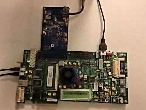
圖9. EVAL-A-INPUT-1AZ評估板和SDP板連接圖
圖10. EVAL-A-INPUT-1AZ評估板電路圖(1)
圖11. EVAL-A-INPUT-1AZ評估板電路圖(2) EVAL-A-INPUT-1AZ評估板材料清單見: 詳情請見: http://www.analog.com/static/imported-files/data_sheets/AD7685.pdf 和 http://www.analog.com/static/imported-files/circuit_notes/CN0213.pdf |